Here, we will start with an example which consists, one of the ways to specifycomplex registers in IDS
Contents
Basic Access Register
Special Access Register
Memory
Interrupt Register
Duplicating Instance
Trigger Buffer Register
Counter Register
Software side Counter Register
Hardware and Software side Counter Register
All type of Counter Register
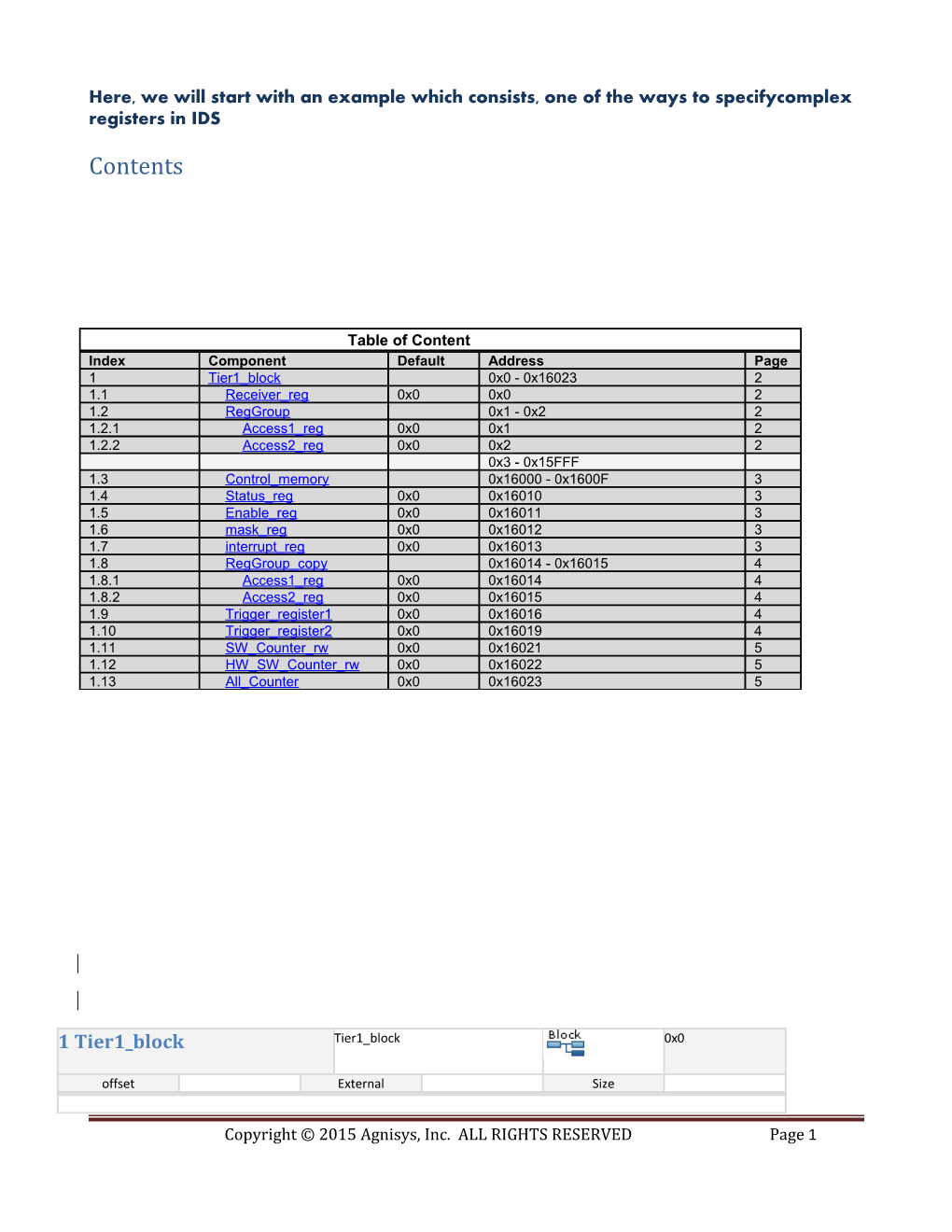
Table of ContentTable of Content
Index / Component / Default / Address / Page
1 / Tier1_block / 0x0 - 0x16023 / 2
1.1 / Receiver_reg / 0x0 / 0x0 / 2
1.2 / RegGroup / 0x1 - 0x2 / 2
1.2.1 / Access1_reg / 0x0 / 0x1 / 2
1.2.2 / Access2_reg / 0x0 / 0x2 / 2
0x3 - 0x15FFF
1.3 / Control_memory / 0x16000 - 0x1600F / 3
1.4 / Status_reg / 0x0 / 0x16010 / 3
1.5 / Enable_reg / 0x0 / 0x16011 / 3
1.6 / mask_reg / 0x0 / 0x16012 / 3
1.7 / interrupt_reg / 0x0 / 0x16013 / 3
1.8 / RegGroup_copy / 0x16014 - 0x16015 / 4
1.8.1 / Access1_reg / 0x0 / 0x16014 / 4
1.8.2 / Access2_reg / 0x0 / 0x16015 / 4
1.9 / Trigger_register1 / 0x0 / 0x16016 / 4
1.10 / Trigger_register2 / 0x0 / 0x16019 / 4
1.11 / SW_Counter_rw / 0x0 / 0x16021 / 5
1.12 / HW_SW_Counter_rw / 0x0 / 0x16022 / 5
1.13 / All_Counter / 0x0 / 0x16023 / 5
1 Tier1_block
/ Tier1_block / / 0x0offset / External / Size
oid=9c041ad0-8d5a-4311-b6a2-2556f3efb1d9
Basic Access Register
1.1 Receiver_reg
/ Receiver_reg / / 0x0offset / external / Size / 32 / default / 0x0
oid=4fd7af35-38db-4eea-b87f-248726d9ceff
Bits / Name / s/w / h/w / Default / Description
7:0 / F1 / Rc / na / 0
8:15 / F2 / ro / rw / 0
31:16 / F3 / rw / rw / 0 / {rtl.hw_w1p=true}A pulse is generated whenever ‘1’ is written to a field through the bus interface
Special Access Register
1.2 RegGroup
/ RegGroup / / 0x1Offset / external / repeat / size
oid=c66a2904-d297-4649-b276-fa64136a5baa
Showing one of the way to use Registers inside RegGroup.
1.2.1 Access1_reg
/ Access1_reg / / 0x1Offset / external / Size / 32 / default / 0x0
oid=64b24d26-2877-4fae-87d2-38ec735da879
Bits / Name / s/w / h/w / default / Description
15:0 / F1 / r/w1c / ro / 0 / H/w readable, s/w write-on-clear.
31:16 / F2 / r/w1s / rw / 0 / H/w read and write, s/w write-to- set.
1.2.2 Access2_reg
/ Access2_reg / / 0x2Offset / external / Size / default / 0x0
oid=7b1dface-2a46-407e-ad8d-ec32a6d7d9fd
Bits / Name / s/w / h/w / default / Description
15:0 / F3 / r/w1s / ro / 0
31:16 / F4 / r/w1c / rw / 0
End RegGroup
Memory
1.3 Control_memory
/ Control_memory / / 0x16000, 0x16001...Offset / 0x16000 / depth / 16 / Width / 32 / default / 1
oid=16844d22-9c41-49e7-80fe-7c8b416e605d
In memory, offset should always be in power of 2.
Interrupt Register
1.4 Status_reg
/ Status_reg / / 0x16010Offset / External / default / 0x0
oid=98c88819-15a0-430a-98b0-a219cae7c6fb
31 / 30 / 29 / 28 / 27 / 26 / 25 / 24 / 23 / 22 / 21 / 20 / 19 / 18 / 17 / 16 / 15 / 14 / 13 / 12 / 11 / 10 / 9 / 8 / 7 / 6 / 5 / 4 / 3 / 2 / 1 / 0
Bits / Name / s/w / h/w / Default / Description
0:0 / F1 / rc / Wo / 0 / {intr.status=1}This interrupt will be enabled by below enable register’s field (F1).
3:1 / F2 / ro / rw / 0
1.5 Enable_reg
/ Enable_reg / / 0x16011offset / External / default / 0x0
oid=fbea7345-c2e6-4c66-94e3-bd40772ef480
31 / 30 / 29 / 28 / 27 / 26 / 25 / 24 / 23 / 22 / 21 / 20 / 19 / 18 / 17 / 16 / 15 / 14 / 13 / 12 / 11 / 10 / 9 / 8 / 7 / 6 / 5 / 4 / 3 / 2 / 1 / 0
Bits / Name / s/w / h/w / Default / Description
0:0 / F1 / rw / rw / 0 / {intr.enable=1}This will enable above register’s interrupthavingsameRHS value of the property.
3:1 / F2 / rw / rw / 0
1.6 mask_reg
/ mask_reg / / 0x16012offset / External / default / 0x0
oid=e892c31b-8762-4826-ac02-213fa521e455
{intr.mask=on}This is the property to use the functionality of mask interrupt.
31 / 30 / 29 / 28 / 27 / 26 / 25 / 24 / 23 / 22 / 21 / 20 / 19 / 18 / 17 / 16 / 15 / 14 / 13 / 12 / 11 / 10 / 9 / 8 / 7 / 6 / 5 / 4 / 3 / 2 / 1 / 0
Bits / Name / s/w / h/w / Default / Description
31:0 / F1 / rw / rw / 0
1.7 interrupt_reg
/ interrupt_reg / / 0x16013offset / External / default / 0x0
oid=d32c1914-7a33-4a91-bb14-aecb4982bc2f
{intr.status=on}This will enable the above interrupt having same RHS value.
31 / 30 / 29 / 28 / 27 / 26 / 25 / 24 / 23 / 22 / 21 / 20 / 19 / 18 / 17 / 16 / 15 / 14 / 13 / 12 / 11 / 10 / 9 / 8 / 7 / 6 / 5 / 4 / 3 / 2 / 1 / 0
Bits / Name / s/w / h/w / Default / Description
31:0 / F2 / r/W1c / wo / 0
Duplicating Instance
This template helps in duplicating or calls any instance from same document or other document.
1.8 RegGroup_copy
/ RegGroup_copy / Ref / 0x16014offset / name / RegGroup / path / type
oid=1845135e-2dcf-4070-a3f7-afb645149225
Trigger Buffer Register
Trigger Buffer Register allows us to use registergreaterthan the bus width and also allows different width register in a document.
(Always place a register template before trigger buffer register template)
1.9 Trigger_register1
/ Trigger_register1 / / 0x16016Offset / buffer_trig / F1 / Size / 96 / endianness / little / default / 0x0
oid=194a2a5b-3820-4e1f-81bd-b2d07a8c37b4
This Trigger register is triggered by field (F1).Currently only “rw” access in supported for s/w and h/w.
Bits / name / s/w / h/w / Default / Description
95:64 / F1 / Rw / Rw / 0
63:32 / F2 / Rw / rw / 0
31:0 / F3 / Rw / rw / 0
1.10 Trigger_register2
/ Trigger_register2 / / 0x16019offset / buffer_trig / F5 / Size / 256 / endianness / little / default / 0x0
oid=e41b7476-8e31-4706-a443-bb88c6169aaf
bits / name / s/w / h/w / default / Description
255:200 / F1 / Rw / rw / 0
199:196 / F2 / Rw / wo / 0
195:96 / F3 / Rw / rw / 0
95:32 / F4 / rw / rw / 0
31:0 / F5 / rw / rw / 0 / This is trigger field.
Note: Trigger Registers are implemented for Verilog output only.
For more information about all this features, please refer to our documentation link.
Counter Register
Counters are use to generate a register which can increment or decrement the value of register depending upon the properties applied to it.
Software side Counter Register
1.11 SW_Counter_rw
/ SW_Counter_rw / / 0x16021offset / external / size / 32 / default / 0x0
oid=797d8eb1-e808-4403-9f13-fb2d04b9e4be
bits / name / s/w / h/w / default / description
5:0 / Fld / rw / na / 0 / {counter.sw.wr=incr,3; counter.sw.rd=decr,3}
Hardware and Software side Counter Register
1.12 HW_SW_Counter_rw
/ HW_SW_Counter_rw / / 0x16022offset / external / size / 32 / default / 0x0
oid=08697177-cd26-4c41-89c5-cec0419bbeba
bits / name / s/w / h/w / default / description
8:0 / Fld / Rw / na / 0 / {counter=incr; counter.decr.thld=6; counter.incr.thld=9; counter.incr.val=2; counter.sw.wr=decr; counter.sw.rd=incr; counter.sat=true}
All type of Counter Register
1.13 All_Counter
/ All_Counter / / 0x16023offset / external / size / 32 / default / 0x0
oid=bee7e6dd-5ed4-4d8d-9437-23d17d18db17
bits / name / s/w / h/w / default / description
21:0 / Fld / rw / ro / 0 / {counter=both; counter.decr.sat=3; counter.incr.sat=90; counter.decr.thld=6; counter.incr.thld=68; counter.decr.val=7; counter.incr.val=2; counter.sw.wr=incr,3; counter.sw.rd=decr,5; counter.precedence=hw,sw_rd,sw_wr}
Copyright © 2015 Agnisys, Inc. ALL RIGHTS RESERVEDPage 1