Ion Implantation in
Silicon Technology
FEATURE by Leonard Rubin and John Poate on implanters are essential to modern integrated-circuit (IC) manufacturing. Doping or otherwise modifying silicon and other semiconductor wafers relies on the technology, which involves generating an ing goes back to the 19th century, and has been continu-
Ially refined ever since. Physicist Robert Van de Graaff of the Massachusetts Institute of Technology and Princeton
University helped pioneer accelerator construction, and the high-voltage technology that emerged from this effort was instrumental in building High Voltage Engineering
Corp. (HVEC) in the late 1940s and 1950s. HVEC served as an incubator for the technology essential to building the first commercial ion implanters and the individuals who pioneered the field.
William Shockley first recognized the potential of ion implantation for doping semiconductor materials, and his 1954 patent application demonstrates a remarkable understanding of the relevant process issues long before implantation entered mass production. However, the patent expired in 1974, just as the commercial ionimplantation market began taking off. So although
Shockley demonstrated visionary insight, his patent earned few royalties. ion beam and steering it into the substrate so that the ions come to rest
Without implanters, beneath the surface. Ions may be allowed to travel through a beam line at the enertoday’s integrated gy at which they were extracted from a source material, or they can be accelerated or decelerated by dc or radio-frequencircuits would be impossible cy (RF) electric fields.
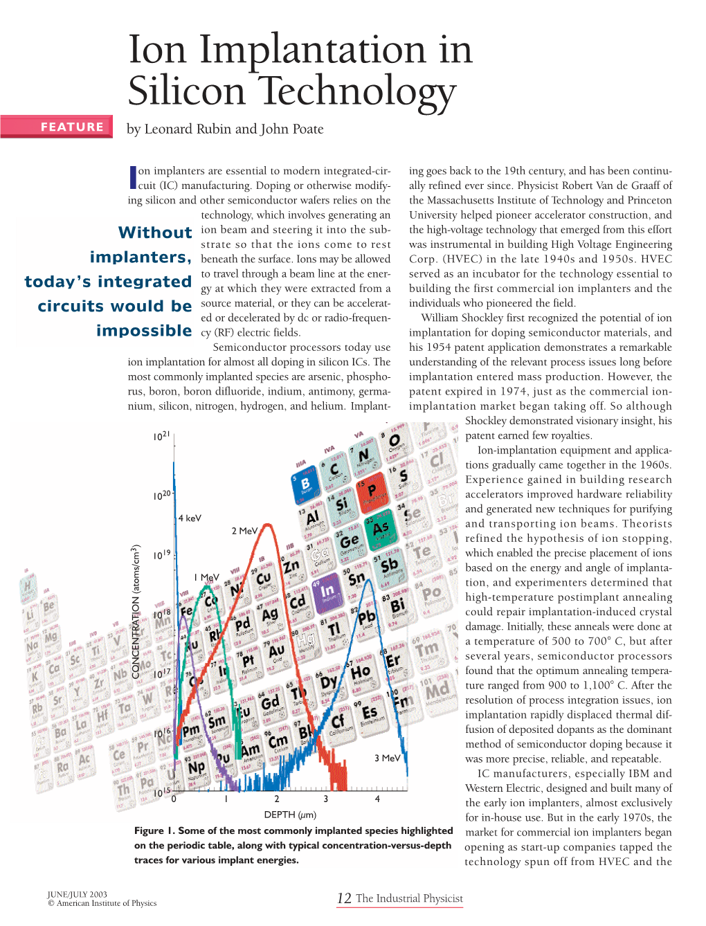
Semiconductor processors today use ion implantation for almost all doping in silicon ICs. The most commonly implanted species are arsenic, phosphorus, boron, boron difluoride, indium, antimony, germanium, silicon, nitrogen, hydrogen, and helium. Implant-
21
10
Ion-implantation equipment and applications gradually came together in the 1960s.
Experience gained in building research accelerators improved hardware reliability and generated new techniques for purifying and transporting ion beams. Theorists refined the hypothesis of ion stopping, which enabled the precise placement of ions based on the energy and angle of implantation, and experimenters determined that high-temperature postimplant annealing could repair implantation-induced crystal damage. Initially, these anneals were done at a temperature of 500 to 700° C, but after several years, semiconductor processors found that the optimum annealing temperature ranged from 900 to 1,100° C. After the resolution of process integration issues, ion implantation rapidly displaced thermal diffusion of deposited dopants as the dominant method of semiconductor doping because it was more precise, reliable, and repeatable.
20
10
4 keV
2 MeV
19
10
1 MeV
18
10
17
10
16
10
3 MeV
IC manufacturers, especially IBM and Western Electric, designed and built many of the early ion implanters, almost exclusively for in-house use. But in the early 1970s, the market for commercial ion implanters began opening as start-up companies tapped the technology spun off from HVEC and the 15
10
01234
DEPTH (µm)
Figure 1. Some of the most commonly implanted species highlighted on the periodic table, along with typical concentration-versus-depth traces for various implant energies.
JUNE/JULY 2003
© American Institute of Physics
The Industrial Physicist
12 17
16
15
14
13
12
11
10
10
10
10
10
10
10
Bonded wafer splitting for silicon on insulator
(H, He)
Polysilicon doping (As, B)
Bipolar buried subcollector (P, As)
Preamorphization
(Ge, Si)
Latch-up/ electrostatic discharge protection
(B)
Source–drain contact
(As, BF , B)
2technology developed by IC manufacturers, who became their customers.
Source–drain extension
Anti
(As, BF , B)
2punch-through
(As, B, In, Sb)
Some memory circuits now sell for less than 20 nanodollars/transistor. Today, implanters and other fabrication hardware must meet aggressive productivity targets to achieve this minuscule cost. A large wafer fabricator may process up to 50,000 wafers/month, with each wafer requiring 20 to 30 implants. This output requires the use of about 20 implanters, each with the capacity to implant more than 200 wafers/h. In practice, maximum implanter throughput typically ranges from
250 to 270 wafers/h, including placing the wafers into and removing them from sealed cassettes used by automated material-handling systems. This throughput is achieved for wafer sizes of 150, 200, and 300 mm.
Depending on the configuration of the beam line and the end station (the wafer-processing chamber), an implanter occupies an area of 16 to 28 m2. Thus, fabrication space poses almost as significant a barrier as capital cost against compensating for poor throughput by installing additional implanters.
CMOS retrograde wells
Channel engineering
(As, BF , P, B, In, Sb)
2
(P, B, As)
Noise isolation wells (P, B)
Threshold voltage adjust
(As, BF , B, P, In)
2
Charge-coupled device wells (B)
0.1 110 100 1,000 10,000
ENERGY (keV)
Figure 2. Dose and energy requirements of major implantation applications (species shown roughly in order of decreasing usage). required 6 to 8 implants, a modern complementarymetal-oxide-semiconductor (CMOS) IC with embedded memory may contain up to 35 implants.
The technique’s applications require doses and energies spanning several orders of magnitude. Most implants fall within one of the boxes in Figure 2. The boundaries of each box are approximate; individual processes vary because of differences in design tradeoffs. Energy requirements for many applications have fallen with increased device scaling. A shallower dopant profile helps keep aspect ratios roughly constant as lateral device dimensions shrink. As energies drop, ion doses usually, but not always, decline as well. The width of the statistical distribution of the implanted ions decreases with energy, and this reduces the dose required to produce a given peak dopant concentration. The result is
Applications
Among semiconductor-processing techniques, ion implantation is nearly unique in that process parameters, such as concentration and depth of the desired dopant, are specified directly in the equipment settings for implant dose and energy, respectively (Figure 1). This differs from chemical vapor deposition, in which desired parameters such as film thickness and density are complex functions of the tun-
Electron confinement beam guide able-equipment settings, which include temperature and gas-flow rate. The number of implants needed to complete an IC has increased as the complexity of the chips has grown. Whereas processing a simple n-type metal oxide semiconductor during the 1970s may have
Dual-slit extraction electrode
Electron confinement beam tunnel
Figure 3.
Flag Faraday
Schematic of the electron confinement technology necessary to transport several milliamperes of beam at energies below 10 keV in a modern high-current beam line.
Selectable resolving housing
Plasma electron flood
(xenon)
Analyzer magnet edge focusing
Deceleration ground extention
Wafer
The Industrial Physicist
13 the sloping lines in Figure 2. Implantation is actually extremely inefficient at modifying material composition.
The highest ion dose implanted with an economical throughput is about 1016/cm2, yet this corresponds to but 20 atomic layers. Only the extreme sensitivity of semiconductor conductivity to dopant concentration makes ion implantation practical.
Ion energy requirements vary from less than 1 keV to more than 3,000 keV. Accelerating ions to higher energies requires a longer beam line, yet low-energy beams are difficult to transport intact over longer distances because the beam cross section expands to a point where it can no longer travel down the beam tube. This funda-
As the name suggests, high-current implanters produce the highest beam currents, up to 25 mA (Figure 3). For high-dose applications, the greater the beam current, the faster the implantation, which means the output of more wafers per hour. Implanter makers have invested a great deal of effort in maximizing beam current, especially at the lowest energies, where Child’s law limits the flux of ions extractablefromasource. Althoughhigh-currentimplanters can produce beams in the 10-µA range, source instabilities make these beams unsuitable for low-dose applications.
The short beam line of these implanters allows an energy range from 1 keV up to 100 to 200 keV.
Medium-current implanters are designed for maximum dose uniformity and repeatability.
Their beam currents are in the range of 1 µA to 5 mA, at energies of 5 to ~600 keV.
The wafer-processing end stations can
Ten radio-frequency resonators
(80 kV @ 13.56 MHz) implant ions at angles up to 60° from the perpendicular to the wafer surface. This is essential for certain applications, such as anti-punchthrough implants, for example, in which dopants must be implanted partially underneath a previously formed gate structure. The lower operational cost of medium-current implanters when used for
Massanalyzing magnet
(70°) lower-dose applications and their ability to do high-tilt implants distinguish them from high-current implanters.
Last, only high-energy implanters can generate megaelectron volt ion beams.
Commercial high-energy implanters produce beam currents for singly-charged ions up to ~1 mA. Energies for multiply-charged ions can be up to ~4,000 keV, with beam
Twelve quadrupole lenses (20 kV dc)
Ten radio-frequency electrodes currents of ~50 µA. High-energy implanters
Figure 4. Schematic of a radio-frequency linear accelerator used in a high-energy ion implanter. mental physics makes it nearly impossible to construct a beam line capable of all required ion energies. Figure 2 indicates that the largest magnitude in required doses occurs in the middle of the energy range. Because dose is essentially the beam’s charge multiplied by the implantation time, available beam currents in the 5- to 200-keV range must vary by at least 4 orders of magnitude to perform all required implants efficiently. This level is difficult to reproduce repeatedly in a single ion-source/beamline configuration. can produce beams down to 10 keV, making them suitable for many medium-current applications as well. This additional functionality justifies the capital cost of these machines. High-energy implanters using both RF linear acceleration (Figure 4) and dc acceleration are used widely today in semiconductor manufacturing.
A modern ion implanter costs about $2–5 million, depending on the model and the wafer size it processes. Of the three classes of implanters, the high-current machines have traditionally been the biggest market in terms of revenue and unit volume. Revenue is increasing faster than unit volume because implanters have become more expensive. However, both revenue and volume are subject to the severe boom-and-bust cycles that have affected the entire semiconductor capital-equipment industry in the past decade, a pattern that will likely continue.
Market segments
Consequently, the commercial ion-implanter market long ago evolved into three segments. The red, black, and blue regions of Figure 2 indicate high-current, medium-current, and high-energy applications, respectively.
The Industrial Physicist
14 Company Location Web site
Axcelis Technologies Beverly, MA
Varian Semiconductor
Equipment Associates
Process requirements
Tokyo, Japan
Gloucester, MA
Horsham, U.K.
The tiny transistor dimensions that allow the fabrication of microprocessors with clock speeds exceeding
3 GHz necessitate strict doping accuracy. For the most sensitive devices, the implanted dose must be as uniform as possible. Typically, a 3-standard-deviation (σ) variation of 1.5% is the acceptable upper limit. This uniformity must be consistently achieved across wafers as large as 300 mm in diameter. Wafer-to-wafer and lot-to-lot repeatability is equally crucial. The energy of the ion beam should not exceed a 3σ variation of 3.0% across all wafers. The angle of the ion beam to the wafer must also be carefully controlled to prevent variations in dopant position at the edge of device features. Variations in dopant depth are also a concern. Implant angle control with a 3σ variation of ~1.0° is usually enough to create reproducible device electrical characteristics.
Applied Materials
Implant Division
Sumitomo Easton Nova
(joint venture with Axcelis)
Nissin Electric Kyoto, Japan
Ibis Technology Danvers, MA
Table 1: Major manufacturers of commercial ion implantation equipment in order of decreasing market share. them remain in service, all ions implanted worldwide at any given time represent a mass transfer of only about
5 mg/s. Two companies located 25 km apart on Boston’s
North Shore, Varian and Axcelis, manufacture roughly
70% of all ion implanters (Table 1). This siting is not entirely coincidental, because many of the same people founded and/or helped build the two companies, Varian in 1971 and Axcelis in 1978. It is unlikely that a significant amount of ion-implanter design will migrate to new areas because of the machines’ complexity. The expertise required to design a new beam line is not easily duplicated, which makes ion implanters the Swiss analog watches of the semiconductor industry. They are an elegant, complex product designed and made mostly by a small number of skilled craftspeople in a small corner of the world.
Designers of modern implanters have largely achieved the desired dose, energy, and angle accuracy. The greatest challenge remaining is to increase the productivity of the beam current at energies below 10 keV. Device scaling has greatly increased the demand for implants in this energy range. Designers also need to reduce implanter-induced contamination as much as possible. Atoms of previously implanted dopants can be sputtered onto the wafer surface (cross-contamination), or ions of the right species but wrong energy or charge state can be implanted (energy contamination). Particles can be deposited onto the wafer surface either by ion-beam transport or during wafer handling. Even particles as small as 120 nm may cause yield losses. Finally, metallic contaminants can be deposited onto the wafer surface, usually from sputtering of beam-line components, or worse, implanted into the wafer (energetic metallic contamination). Modern devices are so sensitive to these problems that many customers demand levels of particle and metallic contamination below those detected by metrology equipment.
Modern end stations implant either one wafer at a time or a small batch of wafers—typically 13 or 17— mounted on a rapidly rotating disk. Only single-wafer end stations are capable of high-tilt implants because of the mechanical complications of supplying water and other necessities to a rotating disk. However, the ability to implant multiple wafers simultaneously gives batch end stations a productivity advantage. Consequently, both end stations have found successful commercial niches. Nearly all medium-current implanters dope a single wafer at a time, and most high-current and highenergy implanters process wafers in batches.
Further reading
Dearnaley, G.; Freeman, J. H.; Nelson, R. S.; Stephen,
J. Ion Implantation; American Elsevier Publishing Co.:
New York, 1973; 802 pp.
Rimini, E. Ion Implantation: Basics to Device Fabrication;
Kluwer Academic Publishers: Boston, 1995; 393 pp.
Rubin, L.; Morris, W. High-Energy Ion Implanters and Applications Take Off. Semiconductor International 1997,
20, 77–85.
Ryssel, H.; Ruge, I. Ion Implantation; John Wiley and Sons: New York, 1986; 350 pp.
Ziegler, J. F., Ed. Ion Implantation: Science and Technology;
Ion Implant Technology Co.: Edgewater, MD, 2000; 687 pp.
Chason, E.; et al. Ion beams in silicon processing and characterization. J. App. Phys. 1997, 81 (10), 6513–6561.
Current, M. I. Ion implantation for silicon device manufacturing: A vacuum perspective. J. Vac. Sci. Tech. A:
W
Vacuum, Surfaces, and Films 1996, 14 (3), 1115–1123.
B I O G R A P H Y
Leonard Rubin (leonard.rubin@axcelis.com) is a senior scientist and John Poate (john.poate@axcelis.com) is vice president and chief technology officer at Axcelis
Technologies in Beverly, Massachusetts.
Makers have shipped more than 6,000 ion implanters worldwide since 1980. Assuming that about 4,000 of The Industrial Physicist
15
Ion Implantation in Silicon Technology